Information magazine of the Department of Industrial Engineering
Università di Trento
Silicon, the second most abundant element in the Earth’s crust after oxygen, is one of the most important semiconductor materials. The reasons for this are to be found in its excellent electrical characteristics and the maturity of its commercial fabrication processes. Owing to this unique properties, silicon-based devices dominate consumer electronics, and have become an indispensable part of modern life.
Beyond everyday applications, silicon also plays a crucial role in a wide range of cutting-edge scientific researches, including space applications and High Energy Physics (HEP) experiments. In collaboration with the Istituto Nazionale di Fisica Nucleare (INFN) and Fondazione Bruno Kessler (FBK), the research group led by Prof. Gian-Franco Dalla Betta has been actively developing advanced 3D silicon sensors for the Large Hadron Collider (LHC) at CERN.
The first use of silicon sensors in HEP experiments dates back to the 1980s. Early prototypes employed n-type silicon substrates with p+ microstrip electrodes on the front surface for signal readout, enabling much more precise reconstruction of particle trajectories, compared with traditional gaseous detectors. By further segmenting the microstrips, pixel detectors were later developed and integrated into major experiments at CERN. However, the highly energetic particles produced in the experiments, as they traverse through the material, can damage silicon sensors. These radiation-induced defects accumulate over time, which eventually lead to severe deterioration of sensor performance. To address the issues, different sensor concepts have been proposed over the years, among which, 3D silicon sensors stand out as the most radiation-hard solution to date.
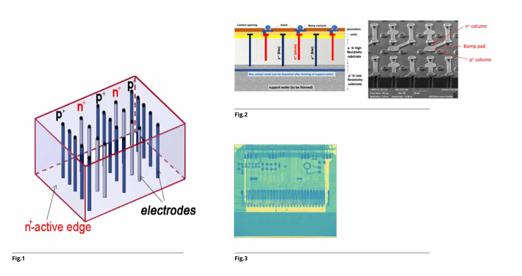
Differently from planar sensors, in which the electrodes are located on the surfaces of the wafer, 3D sensors feature electrodes that penetrate deep into the silicon substrate, as illustrated in Figure 1. In this configuration, the signal charges generated inside the sensor travel much shorter distances before being collected, thereby significantly improving the radiation hardness of the device.
After years of dedicated research and development, 3D silicon sensors designed by Prof. Dalla Betta’s research group at DII and fabricated by FBK were chosen to equip part of the Insertable B-Layer (IBL) of the ATLAS experiment at CERN. This achievement marked a major milestone in the history of 3D sensors, representing their first application in a HEP experiment.
More than a decade of successful operations has demonstrated the outstanding radiation hardness and long-term reliability of the aforementioned 3D sensors, under extreme experimental conditions. To further advance new discoveries and probe the Standard Model with higher precision, the LHC will undergo a major upgrade starting in 2026, entering the High-Luminosity LHC (HL-LHC) era. This upgrade is designed to deliver unprecedented luminosity and extremely high instantaneous particle fluxes, placing stringent requirements on the detector systems. In particular, detectors in the inner layers will need to withstand much higher levels of radiation damage, while providing fast response to distinguish particles originating from different collision events.
To this end, a new type of 3D sensors, called small-pitch 3D pixel sensors, has been developed based on single-sided technology, which largely reduced the pixel size whilst increasing its radiation hardness. Figure 2 (left) shows the schematics of the sensor, Figure 2 (right) presents a scanning electron microscope (SEM) image of the sensor fabricated by FBK, clearly demonstrating the high resolutoon achievable with the fabrication process.
Extensive irradiation campaigns and functional tests have been carried out to evaluate the performance of these sensors over the years. The results demonstrate that they can operate efficiently even after exposure to the highest radiation levels expected for the innermost tracking layers of the HL-LHC. Owing to their outstanding radiation hardness, both the ATLAS and CMS experiments have chosen 3D sensors designed by our group for their innermost detector layers. Figure 3. shows the reconstructed map of the sensor coupled to the readout electronics under X-ray illumination, where different electronic components, such as capacitors and resistors, as well as the routing structures, can be clearly seen.
The HL-LHC upgrade naturally raises the question of the post-HL-LHC era, represented by the proposed Future Circular Collider (FCC). The projected integrated luminosity for such experiments is at least five times higher than that of the HL-LHC, with event pile-up reaching up to 1000 collisions per bunch crossing. To reduce the probability of multiple particles hitting the same pixel simultaneously and to correctly associate particles with their corresponding collisions, a temporal resolution on the order of 10 picoseconds is highly desirable. At the same time, the sensors must be capable of withstanding radiation levels up to ten times higher than those expected at the HL-LHC.
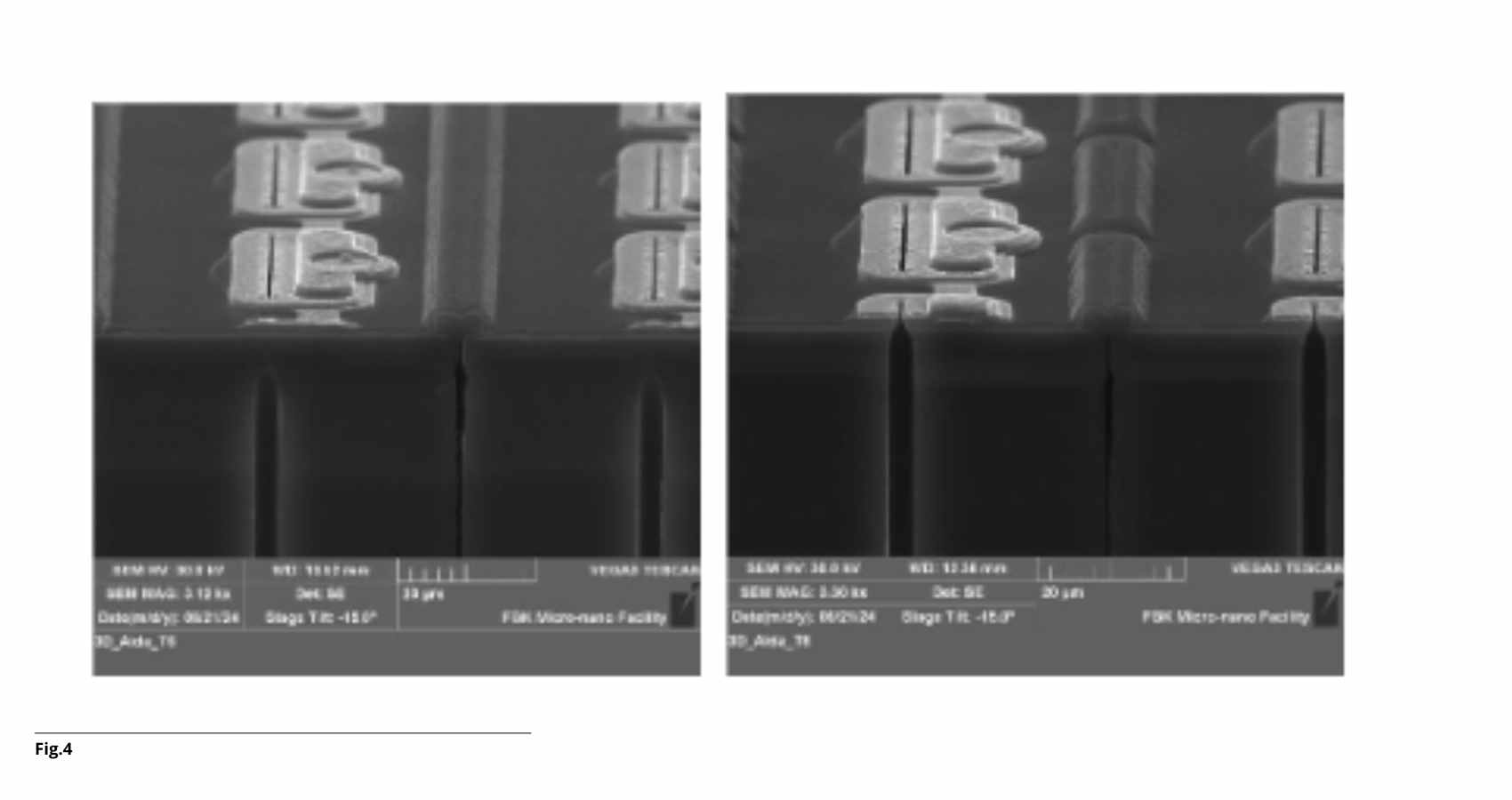
To tackle this particularly challenging problem, our group has also been actively developing the next generation of 3D sensors based on trench-electrode technology. The main motivation behind this approach is that replacing columnar electrodes with trench electrodes enables a much more uniform electric field distribution inside the sensor, thereby improving both timing performance and radiation hardness. Figure 4 shows SEM images of different variants of 3D trench-electrode sensors we designed. Preliminary test results indicate that the sensors can achieve a time resolution of ~10 picoseconds, and no performance degradation has been observed even after exposure to the radiation levels expected at the FCC. These exciting results pave the way for the development of future detector systems for the FCC. Currently, we are working toward improving the fabrication yield of large-area sensors through further optimization of both the sensor design and the fabrication processes, an objective we are optimistic about achieving.
Figure 1. Schematics of columnar-electrode 3D sensors
Figure 2. Schematics of small-pitch 3D pixel sensors (left) and the SEM image of the fabricated sensor (right).
Figure 3. Reconstructed X-ray image obtained using small-pitch 3D pixel sensors.
Figure 4. SEM images of different designs of 3D trench-electrode sensors